LED white light bulb
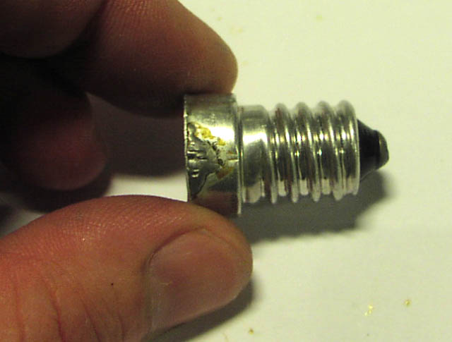 lightbulb was removed outdoor ! and socket cleaned as much as possible
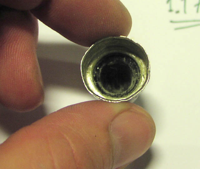 this hole can almost fit some of the components
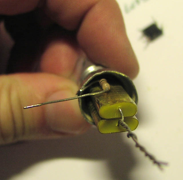 the 100 ohm and 2 x 220nF 400 V types
 the 10uF is a 100V type, so plenty of margin here
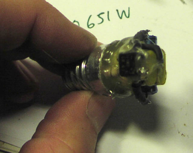 tiny 4 pin rectifier almost visible in the heatmelt glue, yes this thing dont get hot at all !! so heat melt glue can be used.
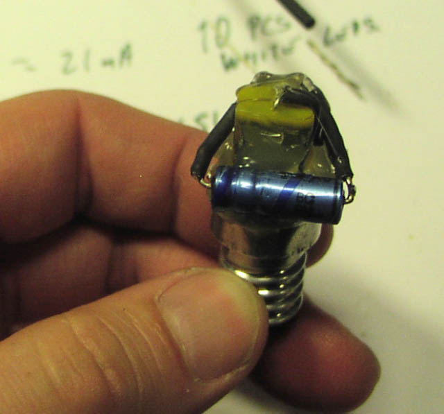
 Try to make it as compact as possible, for better fit in your lamp later
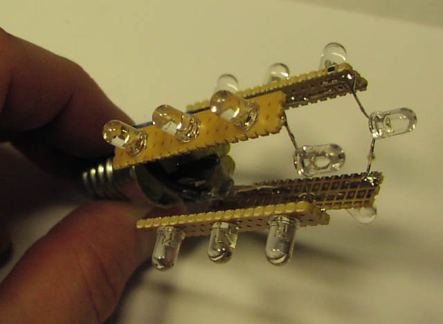
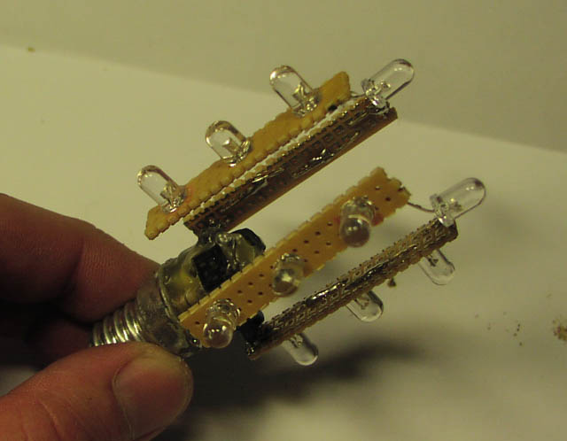
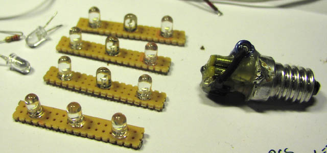 prototype board can be cut out and used as a stable holder for the leds
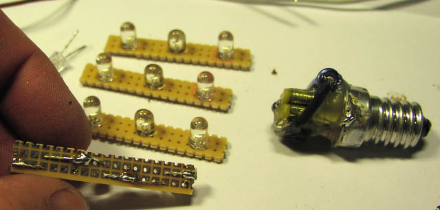 each little board was carefully serial connected and tested again to be sure it is right
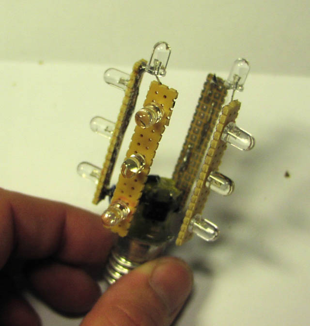 I tried to spread the light in all directions, leds are quite directional specially before I grinded them flat
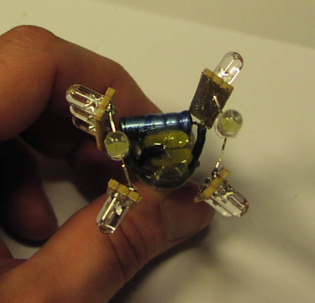 using the capacitor ends as a supply base and the top leds as connections from the 2 and 2 boards, I got all the way arround without adding wires
 making it straight and nice was not my main task, this is only a prototype to prove the NO LOSS supply is good
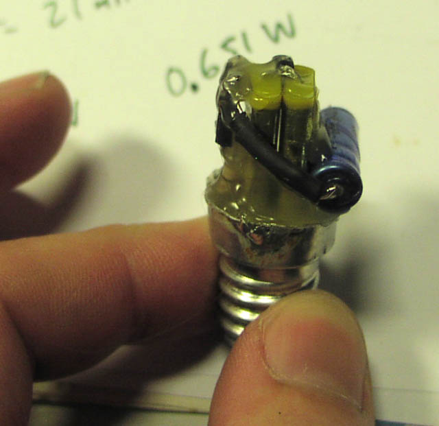
 The 220 ohm resistor can go anywhere in the diode chain, so I added it here and heatshrink'ed it with 2 layers
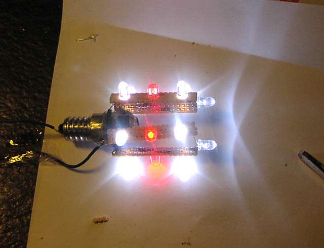 it is clear the red leds are not same hipower technology, just bad luck
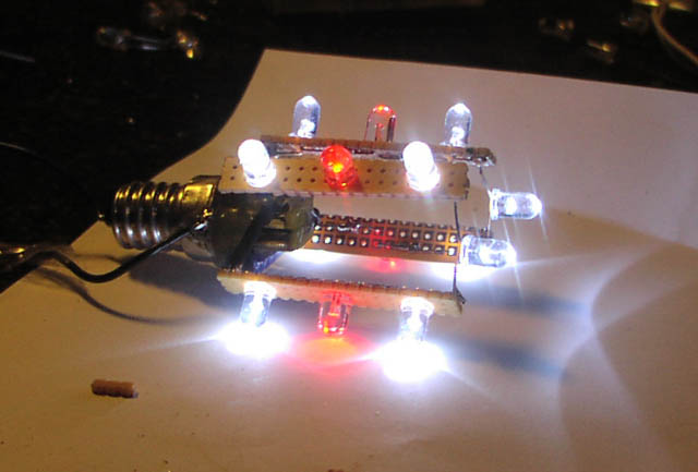 the beam width of the leds is terrible narrow, so to solve this, I simply grinded them flat ! this gives a much more nice diffused light
use sand paper or a table grinder, be carefull not to grind too deep into the led, just make it flat top and stop there.
use sand paper or a table grinder, be carefull not to grind too deep into the led, just make it flat top and stop there.
I feel confident to say anyone can make LED light at home and save big time !

